|
NXP公司的PN512是工作頻率為13.56MHz的高度集成收發器IC,主要用在工作頻率為13.56MHz的無接觸通信,通信距離為50mm.PN512支持四種不同的工作模式: ISO/IEC 14443A/MIFARE 和FeliCa讀/寫器, ISO/IEC 14443B 讀/寫器, ISO/IEC 14443A/MIFARE和FeliCa 卡模式和NFCIP-1模式.通信速率高達424 kbps,器件集成了CRC協處理器,內部有自檢測試和可編程的I/O引腳.本文介紹了PN512主要特性和優勢, 方框圖和多種讀/寫模式框圖, 典型應用電路以及PN51x 演示板電路圖, 和天線間的放大和匹,PCB布局圖與基于PN512的OM5597/RD2612 POS參考設計框圖. The PN512 is a highly integrated transceiver IC for contactless communication at 13.56 MHz. This transceiver IC utilizes an outstanding modulation and demodulation concept completely integrated for different kinds of contactless communication methods and protocols at 13.56 MHz. The PN512 transceiver ICs support 4 different operating modes • Reader/Writer mode supporting ISO/IEC 14443A/MIFARE and FeliCa scheme • Reader/Writer mode supporting ISO/IEC 14443B • Card Operation mode supporting ISO/IEC 14443A/MIFARE and FeliCa scheme • NFCIP-1 mode Enabled in Reader/Writer mode for ISO/IEC 14443A/MIFARE, the PN512’s internal transmitter part is able to drive a reader/writer antenna designed to communicate with ISO/IEC 14443A/ MIFARE cards and transponders without additional active circuitry. The receiver part provides a robust and efficient implementation of a demodulation and decoding circuitry for signals from ISO/IEC 14443A/MIFARE compatible cards and transponders. The digital part handles the complete ISO/IEC 14443A framing and error detection (Parity & CRC). The PN512 supports MIFARE 1K or MIFARE 4K emulation products. The PN512 supports contactless communication using MIFARE higher transfer speeds up to 424 kbit/s in both directions. Enabled in Reader/Writer mode for FeliCa, the PN512 transceiver IC supports the FeliCa communication scheme. The receiver part provides a robust and efficient implementation of the demodulation and decoding circuitry for FeliCa coded signals. The digital part handles the FeliCa framing and error detection like CRC. The PN512 supports contactless communication using FeliCa Higher transfer speeds up to 424 kbit/s in both directions. The PN512 supports all layers of the ISO/IEC 14443B reader/writer communication scheme, given correct implementation of additional components, like oscillator, power supply, coil etc. and provided that standardized protocols, e.g. like ISO/IEC 14443-4 and/or ISO/IEC 14443B anticollision are correctly implemented. In Card Operation mode, the PN512 transceiver IC is able to answer to a reader/writer command either according to the FeliCa or ISO/IEC 14443A/MIFARE card interface scheme. The PN512 generates the digital load modulated signals and in addition with an external circuit the answer can be sent back to the reader/writer. A complete card functionality is only possible in combination with a secure IC using the S2C interface. Additionally, the PN512 transceiver IC offers the possibility to communicate directly to an NFCIP-1 device in the NFCIP-1 mode. The NFCIP-1 mode offers different communication mode and transfer speeds up to 424 kbit/s according to the Ecma 340 and ISO/IEC 18092 NFCIP-1 Standard. The digital part handles the complete NFCIP-1 framing and error detection. Various host controller interfaces are implemented: • 8-bit parallel interface1 • SPI interface • serial UART (similar to RS232 with voltage levels according pad voltage supply) • I2C interface. PN512主要特性和優勢: Highly integrated analog circuitry to demodulate and decode responses Buffered output drivers for connecting an antenna with the minimum number of external components Integrated RF Level detector Integrated data mode detector Supports ISO/IEC 14443 A/MIFARE Supports ISO/IEC 14443 B Read/Write modes Typical operating distance in Read/Write mode up to 50 mm depending on the antenna size and tuning Typical operating distance in NFCIP-1 mode up to 50 mm depending on the antenna size and tuning and power supply Typical operating distance in ISO/IEC 14443A/MIFARE card or FeliCa Card Operation mode of about 100 mm depending on the antenna size and tuning and the external field strength Supports MIFARE 1K or MIFARE 4K emulation encryption in Reader/Writer mode ISO/IEC 14443A higher transfer speed communication at 212 kbit/s and 424 kbit/s Contactless communication according to the FeliCa scheme at 212 kbit/s and 424 kbit/s Integrated RF interface for NFCIP-1 up to 424 kbit/s S2C interface Additional power supply to directly supply the smart card IC connected via S2C Supported host interfaces SPI up to 10 Mbit/s I2C-bus interface up to 400 kBd in Fast mode, up to 3400 kBd in High-speed mode RS232 Serial UART up to 1228.8 kBd, with voltage levels dependant on pin voltage supply 8-bit parallel interface with and without Address Latch Enable FIFO buffer handles 64 byte send and receive Flexible interrupt modes Hard reset with low power function Power-down mode per software Programmable timer Internal oscillator for connection to 27.12 MHz quartz crystal 2.5 V to 3.6 V power supply CRC coprocessor Programmable I/O pins Internal self-test 
圖1.PN512方框圖
圖2.PN512讀/寫模式
圖3.PN512 ISO/IEC 14443 A/MIFARE讀/寫器通信框圖
圖4.PN512 FeliCa讀/寫器模式通信框圖
圖5.PN512 NFCIP-1 模式通信框圖
圖6.PN512 典型應用電路 PN51x 演示板 This document describes the functionality of the demonstration reader based on the PN51x. It includes the functional and electrical specifications and gives the needed details to use this reader as a reference design. This reader implementation is based on the HVQFN32 package of the PN51x device. PN51x 演示板主要特性: • Single 5 V up to 12 V unregulated external power supply • RS232 DSUB9 connector for easy connection to a host PC • Regulated voltage supply for all supply voltages • PN51x Variable Supply Voltage − TVDD = AVDD = DVDD: adjustable, 3.3V or 2.8 V − PVDD: adjustable, 1.8V or equal to DVDD − SVDD: adjustable, 1.8V, 2.8V or 3.3V • NRESET, IRQ signals externally accessible • Support of S2C interface • Analog test signal pins AUX1 and AUX2 • Digital test signal pins D6, D5, D4, D3, D2 and D1 depending on the interface • Breakable line between serial RS232 and PN51x section • Breakable line between serial PN51x and antenna matching section • Breakable line between antenna matching and antenna section • PN51x reader section can be connected via: − Serial UART − I2C − SPI • Antenna size: 33.5 mm x 51.0 mm
圖7.PN51x 演示板電路圖
圖8.PN51x 演示板電路圖:電源
圖9.PN51x 演示板電路圖:天線匹配和天線部分
圖10.PN51x 演示板電路圖:完整的天線電路
圖11.PN51x 演示板PCB布局圖
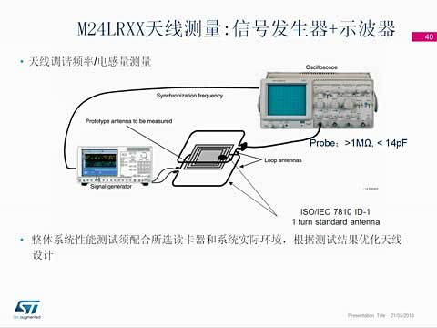
圖12.PN512和天線間的放大和匹配
圖13.PN51x 演示板接收器電路圖 基于PN512的OM5597/RD2612 POS參考設計 OM5597/RD2612 is a reference design of a cost effective EMV compliant Point of Sales Terminal based on NXP components. It provides an EMV Level 1 compliant software stack for contactless as well as contact payment based on PN512/C2 and TDA8026.
圖14.基于PN512的OM5597/RD2612 POS參考設計框圖 詳情請見: http://www.nxp.com/documents/data_sheet/PN512.pdf 和 http://www.nxp.com/documents/application_note/AN1194.pdf |