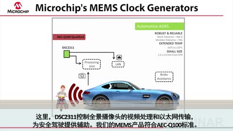
|
Lattice 公司的ispClock 5400D是用于時鐘分配的在系統可編程的超低抖動的零延遲通用扇出的緩沖器,集成了超低抖動時鐘源CleanClock PLL和FlexiClock 輸出區塊,可編程差分輸出標準,單個使能控制: LVDS, LVPECL, HSTL, SSTL, HCSL, MLVDS.主要用在SERDES的低成本時鐘源,ATCA, MicroTCA, AMC, PCI Express以及差分時鐘分配等.本文介紹了ispClock 5400D系列主要特性,功能方框圖,以及ispClock5400D評估板主要特性,電路圖和材料清單(BOM). ispClock 5400D Family In-System Programmable, Ultra-Low Jitter Zero Delay and Fan-Out Buffer,Differential The ispClock5400D family integrates a CleanClock PLL and a FlexiClock Output block. The CleanClock PLL pro-vides an ultra-low-jitter clock source to a set of four V-dividers. The FlexiClock output block receives the clock out-put from these V-dividers through an output switch matrix and distributes them to the output pin using a programmable logic interface. There are two members in the ispClock5400D family, the ispClock5410D (10-output FlexiCLock block) and the ispClock5406D (6-output FlexiClock block). Each of the outputs may be independently configured to support separate I/O standards (LVDS, LVPECL, SSTL, HSTL, MLVDS, HCSL) and output frequency. In addition, the skew of each of the outputs can be independently controlled. All configuration information is stored on-chip in non-volatile E2CMOS® memory. The ispClock5400D devices provide extremely low propagation delay (zero-delay) from input to output using the CleanClock PLL. The PLL VCO output clock frequency is divided down by a set of four V- dividers. The output fre-quencies from these V-dividers, fVCO ÷ 2, fVCO ÷ 4, fVCO ÷ 8 and fVCO ÷ 16 are connected to the output routing matrix. The output routing matrix enables any output pin to derive its clock from any of the V-dividers outputs. Addi-tionally, the reference input clock can be connected directly to any output through the output routing matrix. The FlexiClock block supports dual skew mechanisms: Phase Skew Control and Time Skew Control. These skew control mechanisms enable fixed output clock skew control during power-up and variable skew during operation. The ispClock5400D device can be configured to operate in four modes: zero delay buffer mode, dual non-zero delay buffer mode, non-zero delay buffer mode with output dividers, and combined zero-delay and non-zero delay buffer mode. The I2C interface can be used to dynamically control the ispClock5400D configuration: Output clock frequency, Phase Skew, Time skew, Fan-out buffer mode, Output enable. The core functions of both members of the ispClock5400D family are identical. ispClock 5400D主要特性: CleanClock™ PLL FlexiClock™ I/O Ultra Low Period Jitter 2.5ps Ultra Low Phase Jitter 6.5ps Fully Integrated High-Performance PLL •programmable lock detect •Four output dividers •programmable on-chip loop filter •Compatible with Spread Spectrum clocks •Internal/external feedback Flexible Clock Reference and External Feedback Inputs •programmable differential input reference/feed-back standards - LVDS, LVPECL, HSTL, SSTL, HCSL, MLVDS •programmable termination •Clock A/B selection multiplexer 40 MHz to 400 MHz Input/Output Operation Dual Programmable Skew Per Output •programmable phase adjustment - 16 settings; minimum step size 156 ps-Up to +/- 9.4 ns skew range- Coarse and fine adjustment modes •programmable time delay adjustment - 16 settings; 18 ps Dynamic Skew Control Through I2C Low Output-to-Output Skew (<100ps) Up to 10 Programmable Fan-out Buffers •programmable differential output standards and individual enable controls - LVDS, LVPECL, HSTL, SSTL, HCSL, MLVDS •Up to 10 banks with individual VCCO and GND - 1.5V, 1.8V, 2.5V, 3.3V All I/Os are Hot Socket Compliant Operating Modes •Fan-out buffer with programmable output skew control •Zero delay buffer with dual programmable skew controls Dynamic Reconfiguration through I2C Full JTAG Boundary Scan Test In-System Programming Support Exceptional Power Supply Noise Immunity Commercial (0°to 70℃) and Industrial (-40°to 85℃) Temperature Ranges 48-Pin and 64-pin QFNS Packages ispClock 5400D應用: •Low-cost clock source for SERDES •ATCA, MicroTCA, AMC, PCI Express •Differential Clock Distribution •Generic Source Synchronous Clock Management •Zero-delay clock buffer 
圖1.ispClock 5400D方框圖
圖2.ispClock5410D 功能方框圖
圖3.ispClock5406D功能方框圖 ispClock5400D評估板 This board features an ispClock5406D device that provides in-system-programmable zero delay universal fan-out buffers for use in clock distribution applications. The on-board ispClock5406D is a 6-output clock distribution IC. Differential ultra low skew outputs are organized with two banks per group. Each bank may be independently con-figured to support separate I/O standards (LVDS, LVPECL, HSTL, SSTL, HCSL, and MLVDS) and output fre-quency. In addition, each output provides independent programmable control of phase and time skew. All configuration information is stored on-chip in non-volatile E2CMOS® memory. ispClock5400D評估板主要特性: The ispClock5400D Evaluation Board package includes: • ispClock5400D Evaluation Board – The board features the following on -board components and circuits: ispClock5406D programmable clock (ispPAC-CLK5406D-01SN48I) – Crystal oscillator circuits – Can oscillator circuit landing – Resistor networks – SMA connectors – power jack Test and JTAG interface headers • pre-loaded Base Demo – The kit includes a pre-loaded demo design that highlights key performance character-istics of the ispClock5406D device. • Lattice ispDOWNLOAD™ Cable (HW-USBN-2A)– The ispDOWNLOAD cable provides a hardware connection for in-system programming of the ispClock5406D device. • User’s Guide – Provides information on powering, connecting lab equipment, and using the board as a clock source for various Lattice FPGA evaluation boards. The contents of this user’s guide include demo operation, top-level functional descriptions of the various portions of the evaluation board, descriptions of the on-board con-nectors, switches and a complete set of schematics. • QuickSTART Guide – Provides information on connecting the evaluation board, running the pre-loaded evalua-tion demo.
圖4.ispClock5400D評估板外形圖
圖5.ispClock5400D評估板電路圖(1)
圖6.ispClock5400D評估板電路圖(2)
圖7.ispClock5400D評估板電路圖(3)
圖8.ispClock5400D評估板電路圖(4)
圖9.ispClock5400D評估板電路圖(5)
圖10.ispClock5400D評估板電路圖(6)
圖11.ispClock5400D評估板電路圖(7)
圖12.ispClock5400D評估板電路圖(8)
圖13.ispClock5400D評估板電路圖(9) ispClock5400D評估板材料清單(BOM):
詳情請見:  DS1025[1].pdf
(1.57 MB)
DS1025[1].pdf
(1.57 MB)
來源:網絡 |