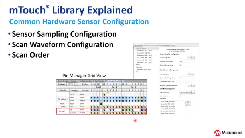
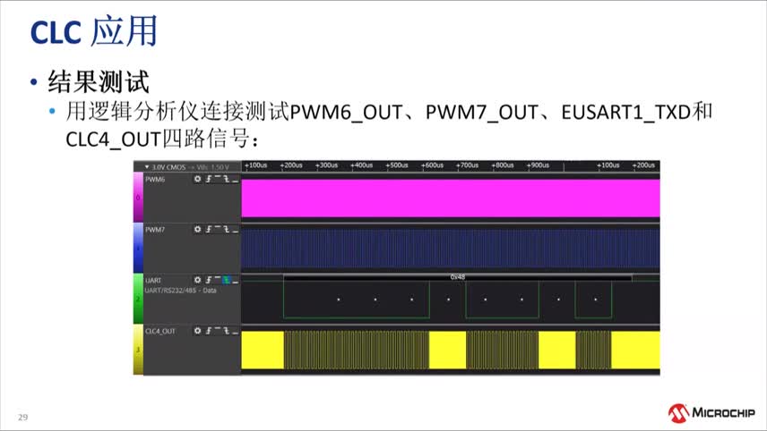
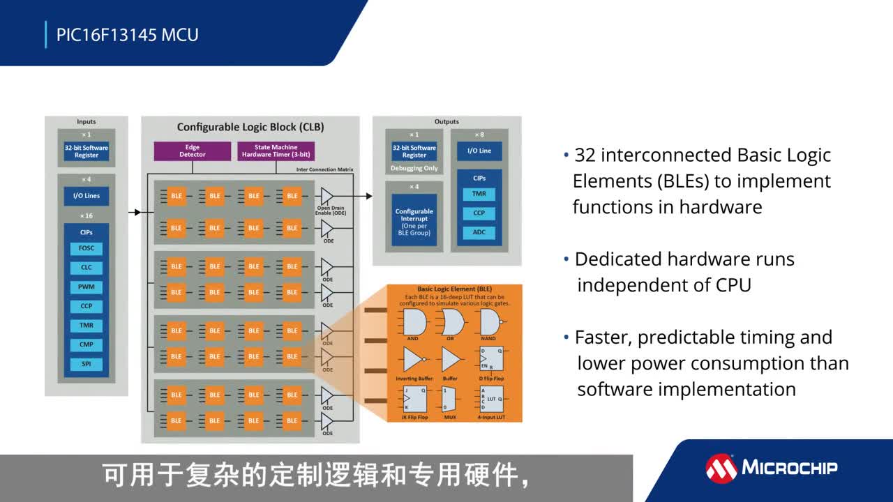
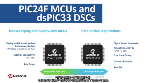
|
Renesas公司的RX210系列是高性能低電壓超低功耗基于32位RX CPU核的閃存MCU,CPU具有73基本指令和9個DSP指令,最大工作頻率50MHz,78DMIPS性能,乘法和除法單元能處理32x32位的運算,具有快速中斷和5級流水線的CISC哈佛架構,片內調試電路,主要用在超低功耗的嵌入式應用.本文介紹了RX210系列主要特性,方框圖以及Renesas入門套件(RSK)主要特性,RSK板布局圖,方框圖和電路圖. The RX210 Group is an MCU with the high-speed, high-performance RX CPU as its core. A variable-length instruction format has been adopted for the RX CPU. Allocating the more frequently used instructions to the shorter instruction lengths facilitates the development of efficient programs that take up less memory. The CPU has 73 basic instructions and and nine DSP instructions, for a total of 82 instructions. It has 10 addressing modes and caters to register–register operations, register–memory operations, immediate–register operations, immediate–memory operations, memory–memory transfer, and bitwise operations. High-speed operation was realized by achieving execution in a single cycle not only for register–register operations, but also for other types of multiple instructions. The CPU includes an internal multiplier and an internal divider for high-speed multiplication and division. The RX CPU has a five-stage pipeline for processing instructions. The stages are instruction fetching, instruction decoding, execution, memory access, and write-back. In cases where pipeline processing is drawn-out by memory access, subsequent operations may in fact be executed earlier. By adopting “out-of-order completion” of this kind, the execution of instructions is controlled to optimize numbers of clock cycles. RX210主要特性: ■ 32-bit RX CPU core Max. operating frequency: 50 MHz Capable of 78 DMIPS in operation at 50 MHz Accumulator handles 64-bit results (for a single instruction) from 32- × 32-bit operations Multiplication and division unit handles 32- × 32-bit operations (multiplication instructions take one CPU clock cycle) Fast interrupt CISC Harvard architecture with 5-stage pipeline Variable-length instructions, ultra-compact code On-chip debugging circuit ■ Low-power design and architecture Operation from a single 1.62- to 5.5-V supply 1.62-V operation available (at up to 20 MHz) Deep software standby mode with RTC remaining usable Four low-power modes ■ On-chip flash memory for code, no wait states 50-MHz operation, 20-ns read cycle No wait states for reading at full CPU speed 128- to 512-Kbyte capacities User code programmable via the SCI Programmable at 1.62 V For instructions and operands ■ On-chip data flash memory Eight Kbytes Erasing and programming impose no load on the CPU. ■ On-chip SRAM, no wait states 20- to 64-Kbyte size capacities ■ DMA DMACA: Incorporates four channels DTC: Four transfer modes ■ ELC Module operation can be initiated by event signals without going through interrupts. Modules can operate while the CPU is sleeping. ■ Reset and supply management Nine types of reset, including the power-on reset (POR) Low voltage detection (LVD) with voltage settings ■ Clock functions Frequency of external clock: Up to 20 MHz Frequency of the oscillator for sub-clock generation: 32.768 kHz PLL circuit input: 4 to 12.5 MHz On-chip low- and high-speed oscillators, dedicated onchip low-speed oscillator for the IWDT Generation of a dedicated 32.768-kHz clock for the RTC Clock frequency accuracy measurement circuit (CAC) ■ Real-time clock Adjustment functions (30 seconds, leap year, and error) Time capture function Time capture on event-signal input through external pins RTC capable of initiating return from deep software standby mode ■ Independent watchdog timer 125-kHz on-chip low-speed oscillator produces a dedicated clock signal to drive IWDT operation. ■ Useful functions for IEC60730 compliance Self-diagnostic and disconnection-detection functions for the AD converter, clock-frequency accuracymeasurement circuit, independent watchdog timer, functions to assist in RAM testing, etc. ■ Up to nine communications interfaces SCI with many useful functions (up to seven interfaces) Asynchronous mode, clock synchronous mode, smart card interface I2C bus interface: Transfer at up to 1 Mbps, capable of SMBus operation (1 interface)RSPI (1) ■ External address space Four CS areas (4 × 16 Mbytes) 8- or 16-bit bus space is selectable per area ■ Up to 14 extended-function timers 16-bit MTU2: input capture, output capture, complementary PWM output, phase counting mode (6 channels) 8-bit TMR (4 channels) 16-bit compare-match timers (4 channels) ■ 12-bit A/D converter Capable of conversion within 1 μs Sample-and-hold circuits (for three channels) Three-channel synchronized sampling available Self-diagnostic function and analog input disconnection detection assistance function ■ 10-bit D/A converter ■ Analog comparator ■ Programmable I/O ports 5-V tolerant, open drain, input pull-up, switching of driving ability ■ MPC Multiple locations are selectable for I/O pins of peripheral functions ■ Temperature sensor ■ Operating temp. range -40 degreeC to +85 degree C 
圖1.RX210方框圖 RX210 系列Renesas入門套件 The Renesas Starter Kit for RX210 is intended as a user-friendly introductory and evaluation tool for the RX210 microcontroller. The board also provides a useful platform for evaluating the Renesas suite of development tools for coding and debugging, using High-performance Embedded Workshop as well as programming the device using E1 emulator and/or Flash Development Toolkit. The Renesas Starter Kit for RX210 may be connected to the host PC using a simple RS232 serial connection or via the included USB E1 on chip debugging interface. The purpose of the board is to enable the user to evaluate the capabilities of the device and its peripherals by giving the user a simple platform on which code can be run only minutes from opening box. It can also prove an invaluable tool in development by providing a useful test platform for code already debugged using one of our more powerful emulation tools.
圖2.RX210 系列入門套件外形圖 RX210 系列Renesas入門套件(RSK)主要特性: This RSK provides an evaluation of the following features: • Renesas microcontroller programming • User code debugging • User circuitry such as switches, LEDs and a potentiometer • Sample application • Sample peripheral device initialisation code The RSK board contains all the circuitry required for microcontroller operation.
圖3.RX210 系列RSK板布局圖
圖4.RX210 系列RSK板頂層元件布局圖
圖5.RX210 系列RSK板方框圖
圖6.RX210 系列RSK板電路圖(1)
圖7.RX210 系列RSK板電路圖(2)
圖8.RX210 系列RSK板電路圖(3)
圖9.RX210 系列RSK板電路圖(4)
圖10.RX210 系列RSK板電路圖(5) 詳情請見:  r01ds0041ej_rx210[1].pdf
(1.49 MB)
r20ut0301eg0300_rskrx210_circuit_diagram[1].pdf
(132.74 KB)
r20ut0302eg0100_rskrx210_usermanual[1].pdf
(1.15 MB)
r01ds0041ej_rx210[1].pdf
(1.49 MB)
r20ut0301eg0300_rskrx210_circuit_diagram[1].pdf
(132.74 KB)
r20ut0302eg0100_rskrx210_usermanual[1].pdf
(1.15 MB)
|