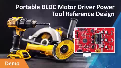
|
NXP公司的LPC2926/2927/2929是集成了ARM968E-S CPU核和工作頻率高達125MHz的兩個TCM區塊,全速USB 2.0 OTG和器件控制器,CAN和LIN,56KB SRAM以及高達768KB閃存,外接存儲器接口,三個10位ADC和多個串行和并行接口。而Hitex公司的BLDC馬達控制板能驅動直流無刷馬達(BLDC)和電壓范圍15V-24V/1A的步進馬達。本文介紹了LPC2926/2927/2929主要特性和優勢,方框圖,以及MCEB-DC馬達控制板框圖,電路圖和PCB元件布局圖。 The LPC2926/2927/2929 combines an ARM968E-S CPU core with two integrated TCM blocks operating at frequencies of up to 125 MHz, Full-speed USB 2.0 OTG and device controller, CAN and LIN, 56 kB SRAM, up to 768 kB flash memory, external memory interface, three 10-bit ADCs, and multiple serial and parallel interfaces in a single chip targeted at consumer, industrial and communication markets. To optimize system power consumption, the LPC2926/2927/2929 has a very flexible Clock Generation Unit (CGU) that provides dynamic clock gating and scaling. LPC2926/2927/2929主要特性和優勢: ARM968E-S processor running at frequencies of up to 125 MHz maximum. Multi-layer AHB system bus at 125 MHz with four separate layers. On-chip memory: Two Tightly Coupled Memories (TCM), 32 kB Instruction TCM (ITCM), 32 kB Data TCM (DTCM). Two separate internal Static RAM (SRAM) instances; 32 kB SRAM and 16 kB SRAM. 8 kB ETB SRAM also available for code execution and data. Up to 768 kB high-speed flash-program memory. 16 kB true EEPROM, byte-erasable and programmable. Dual-master, eight-channel GPDMA controller on the AHB multi-layer matrix which can be used with the Serial Peripheral Interface (SPI) interfaces and the UARTs, as well as for memory-to-memory transfers including the TCM memories. External Static Memory Controller (SMC) with eight memory banks; up to 32-bit data bus; up to 24-bit address bus. Serial interfaces: USB 2.0 full-speed device/OTG controller with dedicated DMA controller and on-chip device PHY. Two-channel CAN controller supporting FullCAN and extensive message filtering. Two LIN master controllers with full hardware support for LIN communication. The LIN interface can be configured as UART to provide two additional UART interfaces. Two 550 UARTs with 16-byte Tx and Rx FIFO depths, DMA support, and RS485/EIA-485 (9-bit) support. Three full-duplex Q-SPIs with four slave-select lines; 16 bits wide; 8 locations deep; Tx FIFO and Rx FIFO. Two I2C-bus interfaces. Other peripherals: One 10-bit ADC with 5.0 V measurement range and eight input channels with conversion times as low as 2.44 μs per channel. Two 10-bit ADCs, 8-channels each, with 3.3 V measurement range provide an additional 16 analog inputs with conversion times as low as 2.44 μs per channel. Each channel provides a compare function to minimize interrupts. Multiple trigger-start option for all ADCs: timer, PWM, other ADC, and external signal input. Four 32-bit timers each containing four capture-and-compare registers linked to I/Os. Four six-channel PWMs (Pulse Width Modulators) with capture and trap functionality. Two dedicated 32-bit timers to schedule and synchronize PWM and ADC. Quadrature encoder interface that can monitor one external quadrature encoder. 32-bit watchdog with timer change protection, running on safe clock. Up to 104 general-purpose I/O pins with programmable pull-up, pull-down, or bus keeper. Vectored Interrupt Controller (VIC) with 16 priority levels. Up to 21 level-sensitive external interrupt pins, including USB, CAN and LIN wake-up features. Configurable clock-out pin for driving external system clocks. Processor wake-up from power-down via external interrupt pins; CAN or LIN activity. Flexible Reset Generator Unit (RGU) able to control resets of individual modules. Flexible Clock-Generation Unit (CGU0) able to control clock frequency of individual modules: On-chip very low-power ring oscillator; fixed frequency of 0.4 MHz; always on to provide a Safe_Clock source for system monitoring. On-chip crystal oscillator with a recommended operating range from 10 MHz to 25 MHz. PLL input range 10 MHz to 25 MHz. On-chip PLL allows CPU operation up to a maximum CPU rate of 125 MHz. Generation of up to 11 base clocks. Seven fractional dividers. Second CGU (CGU1) with its own PLL generates USB clocks and a configurable clock output. Highly configurable system Power Management Unit (PMU): clock control of individual modules. allows minimization of system operating power consumption in any configuration. Standard ARM test and debug interface with real-time in-circuit emulator. Boundary-scan test supported. ETM/ETB debug functions with 8 kB of dedicated SRAM also accessible for application code and data storage. Dual power supply: CPU operating voltage: 1.8 V ± 5 %. I/O operating voltage: 2.7 V to 3.6 V; inputs tolerant up to 5.5 V. 144-pin LQFP package. −40℃ to +85 ℃ ambient operating temperature range. 
圖1。LPC2926/2927/2929方框圖 BLDC馬達控制板 A brushless DC motor consists of a permanent magnetic rotor and solenoids on the stator. Unlike brushed DC motors it provides no built-in commutation system. Therefore an electronically controlled solid state commutation system is required to run the motor. Commutation means alternation of the current flow through the coils and thereby the polarity of the magnetic fields at the right moment – and in the right sequence - to make the rotor turn. The brushless design eliminates the problem of transferring power to the spinning rotor inherent with brushed DC motors and therefore results in better energy efficiency, reduced noise. less maintenance, longer life time and flexible motor control. The MCEB-DC Motor Control Board is intended to be used together with an LPC2929/LPC2939 evaluation board. It connects to the processor board via a 40-pin extension connector which carries the control and sense signals to/from the Motor Control Board. Since the power requirements of the Motor Control Board exceed the capabilities of the evaluation board, an external power supply is required (see specifications below). A BLDC motor is included in the kit and is already mounted on the MCEB-DC board. A datasheet of this motor is available on the installation CD. Alternatively an external motor may be connected to a separate terminal block. This terminal block provides 4 driver outputs which is especially useful for stepper motors. The MCEB-DC allows to run and control the following types of motors: • Brushless DC motor (BLDC) • Stepper motor within a power supply range of 15V to 24V / 1A. The MCEB-DC includes the following building blocks: • Control signal drivers. In the schematics: U200A to U201C. • Motor signal supervisor circuitry with integrated protection. Build up of four half bridge drivers U300 to U303. • 4-phase motor driver stage, build up of 8 power MOSFETS plus additional circuitry for signal shaping and over-voltage protection. In the schematics: Q300A to Q303A and Q300B to Q303B. • Motor sensor signal driver. • Motor current measurement, build up of current sensing ICs U304 to U306 plus shunt resistors R308, R309 and R310. Low pass filters U204A to U206A transfer the PWM output of the current sensor IC to an analog voltage. In addition to its PWM outputs, the current sense IC provides an open drain over current output. These signals from all three ICs are combined as a fault signal. Note that phase 4 has no current sensing circuitry. The motor control signals are driven by PWM (plus width modulation) signals. The source of the PWM signals is the LPC2929/LPC2939. Motor sensor signals (induced voltage and/or hall signals) are fed back to the ADC and GPIO inputs of the microcontroller. In addition, an emergency STOP signal (brake signal) and a temperature sense signal can be connected provided by the current sense circuitry.
圖2。MCEB-DC 馬達控制板外形圖
圖3。MCEB-DC馬達控制板框圖
圖4。LPC2929/39調制和取樣控制子系統方框圖
圖5。MCEB-DC馬達控制板電路圖(1)
圖6。MCEB-DC馬達控制板電路圖(2)
圖7。MCEB-DC馬達控制板電路圖(3)
圖8。MCEB-DC馬達控制板元件布局圖 詳情請見:  LPC2926_27_29[1].pdf
(1.81 MB)
LPC2926_27_29[1].pdf
(1.81 MB)
 nxp_bldc_content.zip
(5.21 MB)
nxp_bldc_content.zip
(5.21 MB)
|