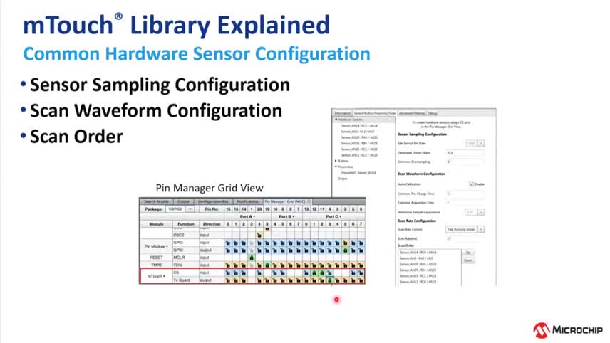
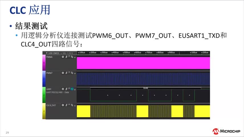
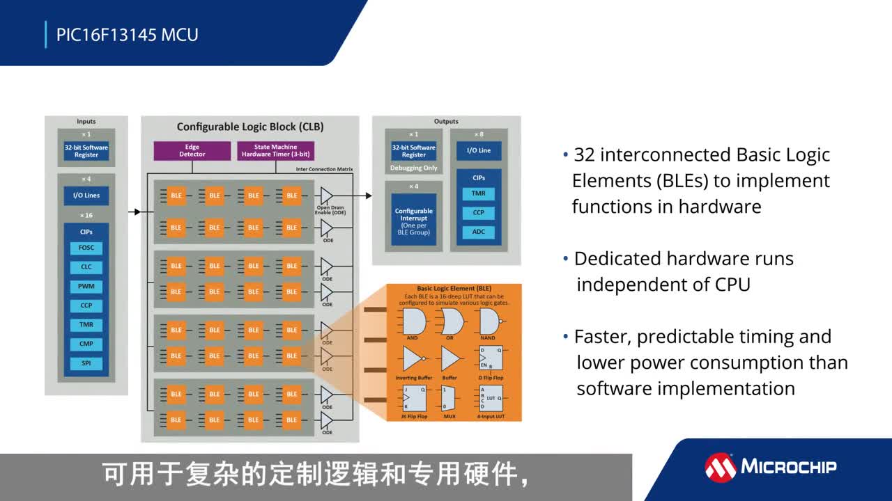
|
On Semi公司的Q32M210是精密的混合信號32位MCU, 集成了2個16位模數轉換器、高精度電壓參考、3個10位數模轉換器和基于ARM® Cortex™-M3 32位內核以及高度可配置的模擬前端及可編程的32位內核和256kB閃存.芯片還集成所有關鍵功能,包括實時時鐘、電源管理、112段液晶顯示屏(LCD)接口、片上低阻抗開關、非限定(uncommitted)運算放大器、精密電壓參考(< 50 PPM/℃)及電阻電容(RC)振蕩器。器件具有高精度感測,可預測工作以及低功耗等特性,主要用于便攜感測應用如病人監測器、無線心電圖機(ECG)和血糖儀等便攜醫療設備.本文介紹了Q32M210主要特性,功能方框圖以及Q32M210評估板主要特性,電路圖和PCB元件布局圖. Q32M210 is a precision, mixed−signal 32−bit microcontroller. The microcontroller is built on the high performance ARMCortex_−M3 processor. The microcontroller incorporates a highly configurable sensor interface designed to work directly with a wide range of sensors having multiple characteristics, including specialized electrochemical sensors. The sensor interface includes dual programmable gain amplifiers, dual 16−bit Analog−to−Digital converters, triple 10−bit Digital−to−Analog converters (for voltage waveform generation and other applications) and three uncommitted, low−noise opamps with configurable signal multiplexing. Flexible connectivity to external non−volatile memory, personal computers, wireless devices, LCD displays and a wide range of other peripherals is enabled by several digital interfaces including I2C, USB (2.0 full−speed compliant) and a high−speed SPI/SQI interface. The microcontroller features flexible clocking options as well as intelligent failure monitoring of power and application interruptions required by high performance, portable, battery operated applications. All necessary clocks including an internal oscillator, real−time clock and a dedicated clock for USB operation are available on−chip (external crystals required for RTC and USB).An embedded power management unit, which incorporates several low power modes, allows application developers to minimize both standby and active power under a wide range of operating conditions. The ultra−low sleep current makes the microcontroller ideal for applications that remain inactive for long periods of time. A large on−chip non−volatile flash memory (256 kB) combined with on−chip SRAM (48 kB) supports complex applications and simplifies application development. The flash contains built−in hardware error checking and correction (ECC) for application reliability. Additionally, a configurable DMA unit which supports independent peripheral−to−memory, memory−to−memory, and memory−to− peripheral channels provides flexible, low power data transfers without processor intervention. A suite of industry−standard development tools, hands−on training and full technical support are available to reduce design cycle time and speed time−to−market. The Q32M210 Microcontroller is Pb−Free, Halogen Free/BFR Free and RoHS Compliant Q32M210主要特性: Ultra Low−  ower and Smart Power Management ower and Smart Power ManagementLess than 400 _A / MHz, up to 16 MHz clock speed Reliable operation down to 1.8 V; 3.3 V nominal supply voltage Ultra−low−current sleep mode with Real−time Clock active (< 750 nA) Low−current standby mode with register and SRAM retention (< 26 _A) Integrated power supplies minimize need for external components. Only a minimum of external passives is required Efficient, Powerful and Robust Processing Architecture 32−bit ARM Cortex−M3 CPU 256 kB on−chip flash with integrated hardware ECC for program and user data storage 48 kB on−chip SRAM Flexible DMA, 4 general−purpose timers, CRC calculator No external voltage required for flash write operation Low−Noise, Low−Leakage, Low−Temperature Drift, Configurable Sensor Interface Triple ultra low−noise opamps with low−leakage inputs and configurable outputs Dual on−chip Programmable Gain Amplifiers (PGA) and ADCs with flexible input multiplexing and wide dynamic range Reconfigurable voltage detection unit Optimal dynamic range scaling of sensor signals Flexible on−chip signal routing for dynamic reconfigurability Minimal temperature drift of gain and offset errors allows for precise calibration Built−in Temperature Sensor Predictable Operation Dedicated brown−out protection circuit prevents execution of code outside of operating range Integrated hardware−based ECC for on−chip flash maintains code and data integrity Watchdog timer High Precision Analog−to−Digital Conversion and Digital−to−Analog Conversion Dual 16−bit ADCs with on−the−fly data rate configurability Triple 10−bit DACs with configurable dynamic range Precision Voltage Reference On−chip, low temperature drift (< 50 ppm/C) voltage reference for ADCs and DACs Flexible On−Chip Clocking rocessor supports speeds up to 16 MHz provided either through internal oscillator or externally supplied clockFlexible Sensor Interconnections Triple low Ron analog multiplexers, including an 8:1 input mux Quad SPST and quad multi−switches for effective simultaneous connection to different sensors USB 2.0 Full−Speed Interface Built−in transceiver for 2.0 Full−speed compatible (12 Mbps) operation with dedicated power supply Flexible External Interfaes Configurable Interface Wakeup pins with configurable pull−ups and pull−downs 8 Configurable GPIO interrupts Dual UARTs, dual SPI, SQI, I2C, PCM (including I2S mode), GPIOs LCD Interface Up to 112 segments with integrated charge pump and backlight driver (up to 10 mA) Packaging Available in 140−pin TLLGA 
圖1.Q32M210功能方框圖 This manual provides detailed information about the configuration and use of the Evaluation and Development Board. The Evaluation and Development Board facilitates prototype system evaluation, hardware verification, and firmware development. The Evaluation and Development Board is designed for use with the software tools included with the Evaluation and Development Kit (EDK) to evaluate the performance and capabilities of the Q32M210 microcontroller. The Evaluation and Development Board enables developers to evaluate the performance and capabilities of Q32M210 in addition to developing, demonstrating and debugging applications. Q32M210評估板包括: • A power supply unit that provides a regulated supply to Q32M210, either from a USB or a 9 V power supply • Access to all peripherals via standard 0.1" headers • An onboard J-Link1 interface for connecting a PC to the Q32M210 ARM Cortex-M3 processor’s JTAG port through USB • An I2C interface compatible with the Philips I2C protocol as described in the Philips I2C-Bus Specification document • A bank of LEDs for monitoring IF4 GPIOs • Five user-defined momentary switches • An onboard 256 kbit SPI EEPROM • An onboard thermistor for temperature measurements • Provisions to populate an optional RS232 transceiver circuit
圖2.Q32M210評估板外形圖
圖3.Q32M210評估板電路配置圖
圖4.Q32M210評估板電路電路圖  32M210電路 32M210電路
圖5.Q32M210評估板電路電路圖  SU/通信電路 SU/通信電路
圖6.Q32M210評估板電路電路圖 32M210模擬接口電路
圖7.Q32M210評估板電路電路圖 32M210模擬開關電路
圖8.Q32M210評估板電路電路圖: IF0-IF3和IF5接口電路
圖9.Q32M210評估板電路電路圖: IF4-LCD接口電路
圖10.Q32M210評估板電路電路圖: IF4-LCD J-鏈接OB SAM電路
圖11.Q32M210評估板電路元件布局圖 詳情請見: http://www.onsemi.cn/pub_link/Collateral/Q32M210-D.PDF 和 http://www.onsemi.cn/pub_link/Collateral/0W674001GEVK_MANUAL.PDF |