電子工程網(wǎng)
標(biāo)題: LMG3410R050功率放大級(jí)解決方案 [打印本頁]
作者: 芻狗 時(shí)間: 2023-9-17 23:23
標(biāo)題: LMG3410R050功率放大級(jí)解決方案
TI公司的LMG3410R050是具有過流保護(hù)的600-V 50-mΩ GaN功率放大級(jí),比硅MOSFET具有固有的優(yōu)勢包括超低輸入和輸出電容,零反向恢復(fù)以降低開關(guān)損耗達(dá)80%之多,以及低開關(guān)節(jié)點(diǎn)振鈴以降低EMI,20ns傳輸時(shí)延用于MHz工作,25-100V/ns用戶可調(diào)轉(zhuǎn)換速率,具有強(qiáng)健的保護(hù),不需要外接保護(hù)元件,主要用在高密度工業(yè)和消費(fèi)類電源,多級(jí)轉(zhuǎn)換器,太陽能逆變器,工業(yè)馬達(dá)驅(qū)動(dòng),不間斷電源(UPS)以及高壓電池充電器.本文介紹了LMG3410R050主要特性, 功能框圖和應(yīng)用電路,以及評(píng)估板LMG3410EVM-018和LMG34xx-BB-EVM主要特性和指標(biāo),電路圖,材料清單和PCB設(shè)計(jì)圖.
The LMG3410R050 GaN power stage with integrated driver and protection enables designers to achieve new levels of power density and efficiency in power electronics systems. The LMG3410’s inherent advantages over silicon MOSFETs include ultra-low
input and output capacitance, zero reverse recovery to reduce switching losses by as much as 80%, and low switch node ringing to reduce EMI. These advantages enable dense and efficient topologies like the totem-pole PFC.
The LMG3410R050 provides a smart alternative to traditional cascode GaN and standalone GaN FETs by integrating a unique set of features to simplify design, maximize reliability and optimize the performance of any power supply. Integrated gate drive enables 100V/ns switching with near zero Vds ringing, <100 ns current limiting self-protects against unintended shoot-through events, Overtemperature shutdown prevents thermal runaway, and system interface signals provide self-monitoring capability.
LMG3410R050 is a high-performance 600-V GaN transistor with integrated gate driver. The GaN transistor provides ultra-low input and output capacitance and zero reverse recovery. The lack of reverse recovery enables efficient operation in half-bridge and bridge-based topologies.
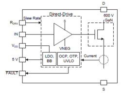
TI utilizes a Direct Drive architecture to control the GaN FET within the LMG3410R050. When the driver is powered up, the GaN FET is controlled directly with the integrated gate driver. This architecture provides superior switching performance compared with the traditional cascode approach.
The integrated driver solves a number of challenges using GaN devices. The LMG3410R050 contains a driver specifically tuned to the GaN device for fast driving without ringing on the gate. The driver ensures the device stays off for high drain slew rates up to 150 V/ns. In addition, the integrated driver protects against faults by providing overcurrent and overtemperature protection. This feature can protect the system in case of a device failure, or prevent a device failure in the case of a controller error or malfunction.
Unlike silicon MOSFETs, there is no p-n junction from source to drain in GaN devices. That is why GaN devices have no reverse recovery losses. However, the GaN device can still conduct from source to drain in 3rd quadrant of operation similar to a body diode but with higher voltage drop and higher conduction loss. 3rd quadrant operation can be defined as follows; when the GaN device is turned off and negative current pulls the drain node voltage to be lower than its source. The voltage drop across GaN device during 3rd quadrant operation is high; therefore, it is recommended to operate with synchronous switching and keep the duration of 3rd quadrant operation at minimum.
LMG3410R050主要特性:
1• TI GaN Process Qualified Through Accelerated Reliability In-application Hard-switching Mission Profiles
• Enables High Density Power Conversion Designs
– Superior System Performance Over Cascode or Stand-alone GaN FETs
– Low Inductance 8mm x 8mm QFN Package for Ease of Design, and Layout
– Adjustable Drive Strength for Switching
Performance and EMI Control
– Digital Fault Status Output Signal
– Only +12 V Unregulated Supply Needed
• Integrated Gate Driver
– Zero Common Source Inductance
– 20 ns Propagation Delay for MHz Operation
– Process-tuned Gate Bias Voltage for Reliability
– 25 to 100V/ns User Adjustable Slew Rate
• Robust Protection
– Requires No External Protection Components
– Overcurrent Protection with <100ns Response
– >150V/ns Slew Rate Immunity
– Transient Overvoltage Immunity
– Overtemperature Protection
– UVLO Protection on All Supply Rails
LMG3410R050應(yīng)用:
• High Density Industrial and Consumer Power Supplies
• Multi-level Converters
• Solar Inverters
• Industrial Motor Drives
• Uninterruptable Power Supplies
• High Voltage Battery Chargers
圖1. LMG3410R050簡化框圖
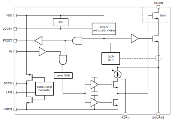
圖2. LMG3410R050功能框圖
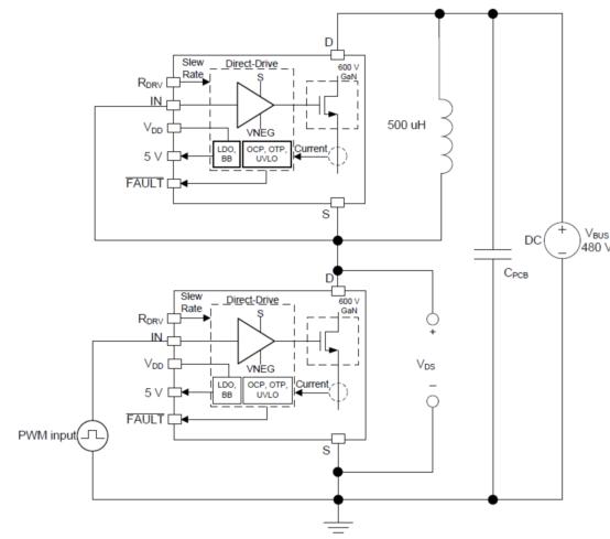
圖3. LMG3410R050用來確定開關(guān)參數(shù)的電路圖
圖4. LMG3410R050應(yīng)用電路圖
評(píng)估板LMG3410EVM-018
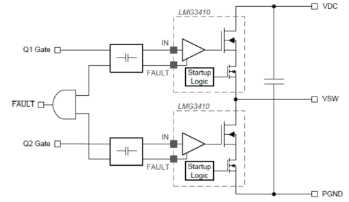
The LMG3410EVM-018 features two LMG3410R050 600V GaN power transistors with integrated drivers that are configured in a half bridge with all the required bias circuit and logic/power level shifting. Essential power stage and gate driving high frequency current loops are fully enclosed on the board to minimize parasitic inductances, reducing voltage overshoots and improving performance. The LMG3410EVM-018 is configured to have a socket style external connection for easy interface with external power stages to run the LMG3410R050 in various applications.
圖5.評(píng)估板LMG3410EVM-018簡化電路
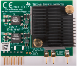
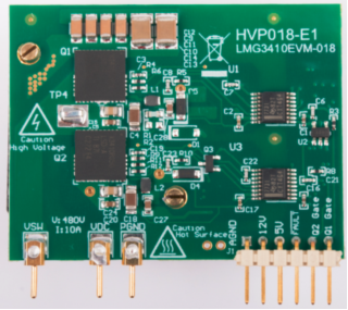
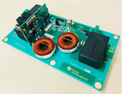
圖6.評(píng)估板LMG3410EVM-018外形圖(頂視)
圖7.評(píng)估板LMG3410EVM-018外形圖(底視)
評(píng)估板LMG3410EVM-018主要特性和指標(biāo):
• Two options to bias the LMG3410, isolated power or from bootstrap diode
• Over temperature, overcurrent, and under voltage lockout protection with FAULT indication that is level shifted to an AGND referenced signal
• Gate logic input support of either 3.3V or 5V logic
• Maximum recommended operating voltage of 480V and absolute maximum voltage of 600V買元器件現(xiàn)貨上唯樣商城��!
評(píng)估板LMG34xx-BB-EVM主要特性和指標(biāo):
• Requires only a single 12V bias supply
• Requires only a single 0V to 5V PWM input to generate gate drive signal
• PWM disable in the event of a fault from the LMG3410EVM-018
• Maximum recommended operating voltage of 480V and absolute maximum voltage of 600V
• Maximum recommended operating inductor current of 8A
The LMG3410EVM-018 is designed for use in AC/DC, DC/DC and DC/AC applications
• Totem-Pole PFC converters
• Phase-Shifted Full Bridge or LLC Converter
• Buck converter such as the LMG34XX-BB-EVM
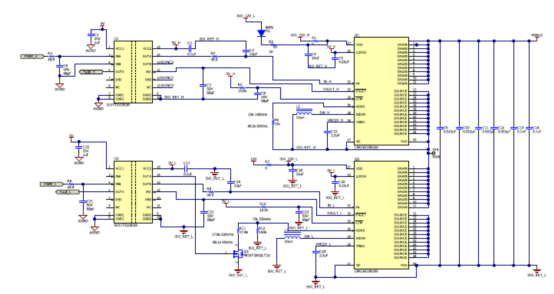
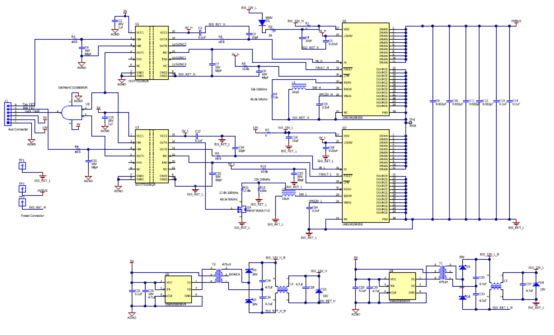
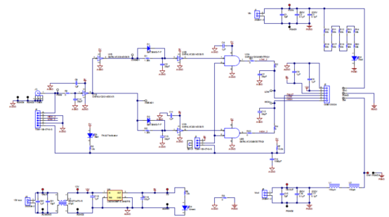
圖8.評(píng)估板LMG3410EVM-018電路圖
圖9.評(píng)估板LMG34xx-BB-EVM電路圖
圖10. 評(píng)估板LMG3410EVM-018和LMG34XX-BB-EVM連接圖
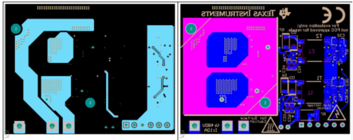
圖11. 評(píng)估板LMG3410EVM-018 PCB設(shè)計(jì)圖:左:內(nèi)部銅層2;右:底層和元件
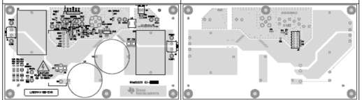
圖12. 評(píng)估板LMG34XX-BB-EVM PCB設(shè)計(jì)圖:左:頂層和元件;右:底層和元件
| 歡迎光臨 電子工程網(wǎng) (http://m.qingdxww.cn/) |
Powered by Discuz! X3.4 |
主站蜘蛛池模板:
好男人好手机视频在线影视
|
国产成人精品一区二区三在线观看
|
欧美综合第一页
|
日本高清va不卡视频在线观看
|
四虎永久地址
|
亚洲欧洲日产国码一级毛片
|
欧美大香线蕉线伊人图片
|
国产精品不卡在线
|
成人一级黄色大片
|
草草青青
|
国产精品久久久久久久专区
|
香蕉国产线观看
|
在线精品视频在线观看高清
|
四虎影院在线观看免费
|
英语课强插英语课代表
|
青青青国产免费手机视频在线观看
|
国产亚洲自拍一区
|
欧美三级在线看
|
麻豆高清在线
|
性做久久久久久久免费看
|
久久国产精品99久久久久久老狼
|
日本在线高清视频
|
色网站在线
|
国产又色又爽又黄的网站在线一级
|
羞羞午夜
|
白色强人粤语版在线观看港剧网
|
青青草97国产精品免费观看
|
污片网站|
欧美bbbxxx
|
欧美一区二区三区gg高清影视
|
奇米一二区
|
岛田阳子五十路在线观看
|
欧美日韩精选
|
国产99久久
|
综合精品一区
|
麻豆国产精品有码在线观看
|
干一干操一操
|
国产羞羞网站
|
亚洲另类视频
|
亚洲视频h
|
欧美日韩在线播放一区二区三区
|